Paper gets a cover in IOP Nanotechnology
by Mikhail Ladanov on Oct.03, 2013, under Uncategorized

Recently published paper Microfluidic hydrothermal growth of ZnO nanowires over high aspect ratio microstructures is now featured on the cover of September issue of Volume 24 IOP Nanotechnology
False Color SEM image of a fly
by Mikhail Ladanov on May.24, 2011, under SEM pictures
It’s been a while since I posted something here, and I surely have a lot of interesting stuff to show, but before everything else I’d like to show this false color SEM image of a fly, specifically, its eye and some area around it. Three SEM images were taken at 30, 20 and 10 kV to serve as three color channels for this RGB image. Some post processing was also applied. One can see that some of the antennae were bent at different angle at different accelerating voltages, causing these color artifacts. Sorry, can’t do anything with that. Nex time I’ll try to choose more… stable sample.

Patterned ZnO nanowires
by Mikhail Ladanov on Jul.01, 2010, under SEM pictures
Keep growing ZnO nanowires by hydrothermal method. I pattern them using microcontact printing of the seeding solution

Controlled growth of ZnO nanowires using microcontact printing
by Mikhail Ladanov on May.25, 2010, under SEM pictures
I was posting some time ago about microcontact printing of seeding layer for controlled growth of the ZnO nanowires. Here we go. The first sample and I can see some lines of ZnO NW growing on the substrate.

Strange sphere
by Mikhail Ladanov on May.25, 2010, under SEM pictures
This is just some strange looking sphere, probably ZnO, that I bumped into while investigating one of my samples.

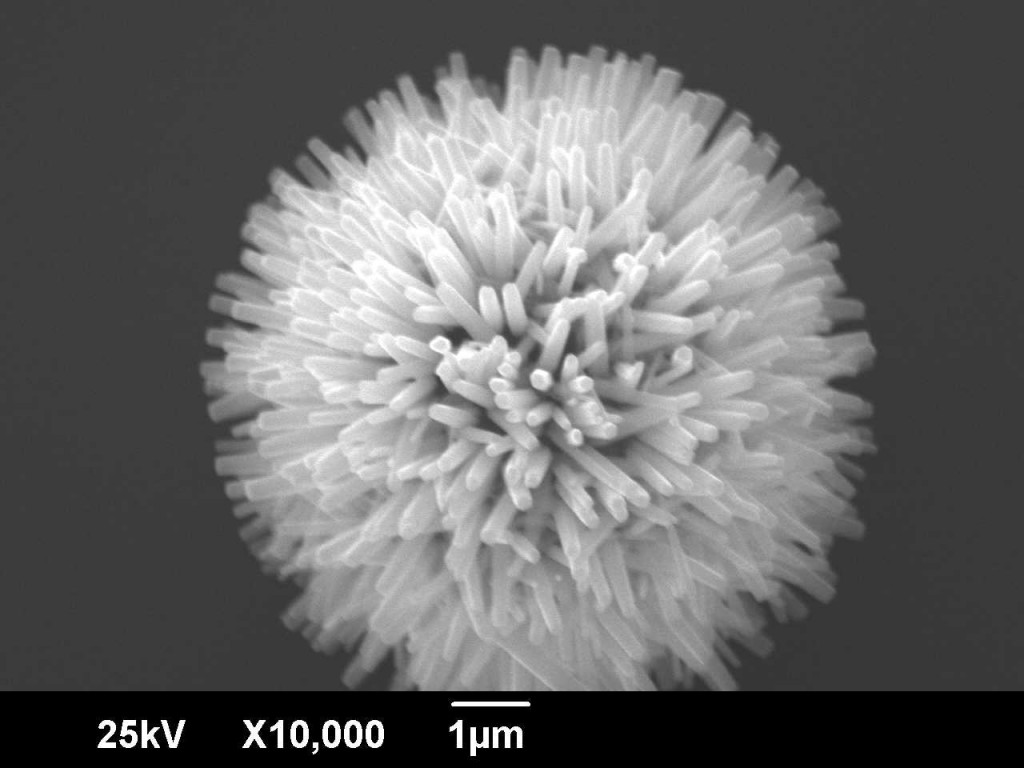
The Hedgehog
by Mikhail Ladanov on May.25, 2010, under SEM pictures
This is a cluster of ZnO nanowires. For ZnO NW to grow one generally need to create a seeding layer consisting of nanocrystalline ZnO. It can be done by depositing solution of zinc acetate in ethanol and annealing substrate at 300°C. If there is a particle on the surface of the substrate, surface tension can draw the solution to this particle, leaving area around without any seeding layer. In my opinion this “hedgehog” was formed around such a particle, while the area around it is without any ZnO NW. there are nanwires of expected shape and geometry father away from this structure.

Stamp for microcontact printing
by Mikhail Ladanov on Mar.19, 2010, under AFM images
This is an AFM image of a stamp made from polymer. I want to try it for microcontact printing of seeding layer for ZnO NW growth.

ZnO nanowires
by Mikhail Ladanov on Mar.15, 2010, under SEM pictures
I was trying to grow ZnO nanowires using a new set up, but apparently messed up somewhere putting the seeding layer on the surface. In this picture, as far as I can tell, ZnO nanowires grew around a ZnO nanocrystall. Though the form and the shape of nanowires are what I was looking for, I’d rather have them growing from the susbtrate.
Chemically grown ZnO NWs
by Mikhail Ladanov on Feb.16, 2010, under Recipe, SEM pictures
Forest of chemically grown ZnO nanowires. Solution was 5 mM/L of Hexamethylenetetramine and Zinc Nitrate in water at 90 °C. Substrate was seeded with ZnO nanocrystalline by dropcasting of 0.5 mM/L of Zinc Acetate Dihydrate in ethanol and consecutive annealing at 350 °C. SEM image is tilted 45°.

AFM set up
by Mikhail Ladanov on Feb.16, 2010, under Photos
AFM set up in Dr. Matthews laboratory, Department of Physics. Small, light, yet powerful. Easy to use.
